Tradução e análise de palavras por inteligência artificial ChatGPT
Nesta página você pode obter uma análise detalhada de uma palavra ou frase, produzida usando a melhor tecnologia de inteligência artificial até o momento:
- como a palavra é usada
- frequência de uso
- é usado com mais frequência na fala oral ou escrita
- opções de tradução de palavras
- exemplos de uso (várias frases com tradução)
- etimologia
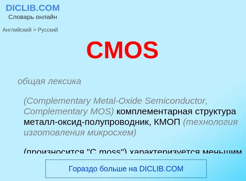
CMOS - tradução para russo
общая лексика
(Complementary Metal-Oxide Semiconductor, Complementary MOS) комплементарная структура металл-оксид-полупроводник, КМОП (технология изготовления микросхем)
(произносится "C moss") характеризуется меньшим быстродействием, но высокой плотностью размещения элементов и малым потреблением энергии
существительное
общая лексика
комплементарный металло-оксидный полупроводник
синоним
общая лексика
CMOS-память
небольшая микросхема на системной плате ПК, содержащая от 128 до 256 байт энергонезависимой памяти с параметрами конфигурации ПК и временем внутренних часов
ОЗУ, выполненное по технологии CMOS
Смотрите также
микроэлектроника
КМОП ИС с монолитной подложкой
Wikipédia
Complementary metal–oxide–semiconductor (CMOS, pronounced "sea-moss", /siːmɑːs/, /-ɒs/) is a type of metal–oxide–semiconductor field-effect transistor (MOSFET) fabrication process that uses complementary and symmetrical pairs of p-type and n-type MOSFETs for logic functions. CMOS technology is used for constructing integrated circuit (IC) chips, including microprocessors, microcontrollers, memory chips (including CMOS BIOS), and other digital logic circuits. CMOS technology is also used for analog circuits such as image sensors (CMOS sensors), data converters, RF circuits (RF CMOS), and highly integrated transceivers for many types of communication.
The CMOS process was originally conceived by Frank Wanlass at Fairchild Semiconductor and presented by Wanlass and Chih-Tang Sah at the International Solid-State Circuits Conference in 1963. Wanlass later filed US patent 3,356,858 for CMOS circuitry and it was granted in 1967. RCA commercialized the technology with the trademark "COS-MOS" in the late 1960s, forcing other manufacturers to find another name, leading to "CMOS" becoming the standard name for the technology by the early 1970s. CMOS overtook NMOS logic as the dominant MOSFET fabrication process for very large-scale integration (VLSI) chips in the 1980s, also replacing earlier transistor–transistor logic (TTL) technology. CMOS has since remained the standard fabrication process for MOSFET semiconductor devices in VLSI chips. As of 2011, 99% of IC chips, including most digital, analog and mixed-signal ICs, were fabricated using CMOS technology.
Two important characteristics of CMOS devices are high noise immunity and low static power consumption. Since one transistor of the MOSFET pair is always off, the series combination draws significant power only momentarily during switching between on and off states. Consequently, CMOS devices do not produce as much waste heat as other forms of logic, like NMOS logic or transistor–transistor logic (TTL), which normally have some standing current even when not changing state. These characteristics allow CMOS to integrate a high density of logic functions on a chip. It was primarily for this reason that CMOS became the most widely used technology to be implemented in VLSI chips.
The phrase "metal–oxide–semiconductor" is a reference to the physical structure of MOS field-effect transistors, having a metal gate electrode placed on top of an oxide insulator, which in turn is on top of a semiconductor material. Aluminium was once used but now the material is polysilicon. Other metal gates have made a comeback with the advent of high-κ dielectric materials in the CMOS process, as announced by IBM and Intel for the 45 nanometer node and smaller sizes.


